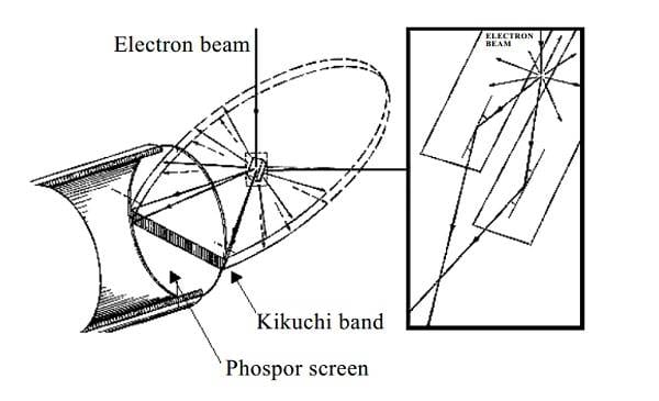
1 IntroductionThe history of electron backscatter diffraction (EBSD) should be traced back to the band-shaped diffraction pattern seen by Kikuchi in a transmission electron microscope in 1928, the Kikuchi line, although this Kikuchi line is transmitted electronically. Until 1954, Alam, Blackman, and Pashley also used transmission electron microscopy to film the wide-angle kikuchi patterns cleaving LiF, KI, NaCl, PbS2 crystals from film, the first strictly electronic backscatter diffraction. In 1973, Venables and Harland conducted a crystallographic study of the material using electron backscatter diffraction patterns on scanning electron microscopy, opening up the application of EBSD in materials science. In the late 1980s, Dingley used screens and television cameras to receive and acquire electron backscatter diffraction patterns. In the 1990s, automatic patterning was achieved. With the rapid development of digital cameras, computers and software, the current product EBSD has realized the full automation from pattern reception and collection to calibration. Can get more than 100 frames per second Kikuchi pattern and calibration results, widely used in geology, microelectronics, materials science and so on.2 The formation principle of EBSD and its contained physical meaningElectronic backscatter diffractometer is usually installed on the SEM or electronic probe. The sample surface and the horizontal is about 70 °. When the incident electron beam enters the sample, it will be scattered by the atoms in the sample. A considerable part of the electrons escape the sample surface due to the scattering angle. This part of the electron is called backscattered electron. Backscattered electrons in the process of leaving the sample with a sample family of crystal face meet the Bragg diffraction condition 2dsinθ = λ that part of the diffraction of the diffraction to form two vertices for the scattering point, and the crystal plane perpendicular to the two conical surfaces, Two conical surface and the receiving screen after the formation of a cross-section of the bright band, the Kikuchi band. The center line of each kikuchi zone corresponds to the cross-section of the plane where the Bragg diffraction occurs from the scattering point of the electron on the sample and the receiving screen, as shown in FIG. 1. An electron backscatter diffraction pattern is called an electron backscatter diffraction pattern (EBSP). An EBSP often contains more than one Kikuchi band. Receive screen received EBSP Digitized by a CCD digital camera and sent to a computer for calibration and calculation. It is worth noting that the EBSP comes from a thin layer of about a few tens of nanometers below the surface of the sample. The deeper electrons, although Bragg diffraction may also occur, may be further scattered by atoms to change the direction of motion as they further exit the sample surface, eventually becoming the backs of EBSPs. Therefore, electron backscatter diffraction is a surface analysis method. Second, the reason why the sample is tilted about 70 ° is that the larger the tilt angle is, the more backscattered electrons are formed and the stronger the EBSP pattern is formed. However, a large tilt angle will lead to the electron beam positioning in the sample surface is not allowed to reduce the sample The spatial resolution of the product surface and other negative effects, so now the EBSD tilt the sample about 70 °.Figure 1 EBSD formation principleThe electron backscatter diffraction pattern contains four sample-related information: crystal symmetry information; crystal orientation information; crystal integrity information; lattice constant information.Figure 2 shows a typical EBSP pattern obtained by the author.The pattern contains several Kikuchi bands corresponding to different crystal faces.Only the crystal family with non-zero structural factor will undergo Bragg diffraction to form the Kikuchi band, while the crystal family with zero structural factor will not form the Kikuchi band due to the zero diffraction intensity. Kikuchi different Kikuchi intersect with the formation of Kikuchi. Because Kikuchi corresponds to crystal plane family, Kikuchi is equivalent to the common direction of each crystal family corresponding to each Kikuchi band, that is, the direction of crystal axis. As can be seen from Figure 2, Kikuchi very rotational symmetry. This rotational symmetry is directly related to the symmetry of the crystal structure. Specifically, the rotational symmetry corresponding to the corresponding crystal axis adds center symmetry, that is, 2-rotation symmetry. Such as the cubic crystal [111] direction for the three rotation symmetry, and the EBSP pattern [111] Kikuchi very six symmetry. Symmetry of crystal structure can be divided into 230 kinds of space group. The electron backscatter diffraction pattern formed by Bragg diffraction can not distinguish between the symmetrical operation components in space group and the same diffraction intensity due to the same structural factor of (h, k, l) and (-h, -k, -l) The introduction of the second rotation symmetry, EBSP can not distinguish between the 32 kinds of point group, only can distinguish between the two kinds of rotational symmetry of 11 Laue group. In other words, EBSP patterns can only have 11 different rotational symmetries.Figure 2 Ni typical EBSP patternAs mentioned above, the center line of each Kikuchi zone is equivalent to the cross-sectional line of the receiving screen after the corresponding crystal surface of the sample is irradiated with the electron beam. Each Kikuchi electrode corresponds to the extension of the corresponding crystal plane at the electron beam irradiation and The acceptance screen is formed by intercept, therefore, the EBSP contains the crystallographic orientation information of the sample. The crystal orientation of the sample can be calculated by the single kikuchi or triple kikuchi method under the condition of the sample placement, the location of the incident electron beam and the geometry of the receiving screen.The integrity of the lattice is clearly related to the quality of the EBSP pattern. When the crystal lattice is intact, the edges of the Kikuchi band in the EBSP pattern formed are sharp, and even high-order diffraction can be observed (as shown in FIG. 2); when the lattice undergoes severe deformation and causes defects such as distortion and distortion of the crystal lattice and a large number of dislocations Kikuchi edge fuzzy, diffuse (Figure 3). The reason is because the Kikuchi band formed by the Bragg diffraction, reflecting the atomic periodic arrangement of information, the more complete the crystal, the higher the Bragg diffraction intensity, the more sharp the edge of the formation of Kikuchi band.Figure 3 Deformed titanium alloy EBSP patternAs can be seen from Figure 1, the width of the Kikuchi W crystal lattice spacing and the corresponding d between the surface has the following relationship:W = R · θ (1)λ = 2dsinθ (2)Where R is the distance between the Kikuchi band on the receiving screen and the point of incidence of the electron beam on the sample, and λ is the wavelength of the incident electron beam.3 EBSD in materials research3.1 Grain orientation, grain orientation distribution (micro-texture), orientation and customary determination of habitThe pattern received by the EBSD screen is collected by the CCD digital camera and sent to the computer. The computer performs Hough transform to detect the position of each Kikuchi band and calculates the angle between the Kikuchi bands. Then, Angle theory to compare the values of Kikuchi and Kikuchi. Figure 4 shows a calibrated EBSP pattern. In the figure, “10” indicates the center of the receiving screen, that is, the intersection of the incident position of the electron beam on the sample and the receiving screen vertical line on the screen. If the position of the electron beam on the sample is known to be perpendicular to the screen, the crystallographic orientation of the grains can be calculated using a single kikuchi or triple kikuchi method. By carefully setting the test conditions, the absolute accuracy of the EBSD determination of crystal orientation can be ≤ 0.25 °. If the electron beam in the sample at a certain distance for a little EBSP pattern, a certain area on the surface of the sample mapping, you can determine the polycrystalline sample orientation of each grain, the statistical calculation, you can determine the statistical distribution of crystal orientation – Texture. Due to the rapid development of CCD cameras, computers and software, the new EBSD can measure EBSP patterns very fast and give the result of grain orientation. For example, Crystal of England’s Oxford can collect more than 100 EBSP patterns per second and give the orientation results. Up to 512 × 384 dots can be measured in one field of view of the sample. By varying the magnification, we can determine the texture on the sample from mm2 to μm2 area. The spatial resolution of EBSD is generally about 0.5μm. If installed on a field emission scanning electron microscope, the spatial resolution can be less than 10 nm. Therefore, the orientation of nm grains can be determined with EBSD. The texture measured at high magnification is often referred to as microdomains. At the same time, EBSD can also be used to measure large-area macroscopic textures. After measuring the texture of the adjacent area at low magnification, the montage method is used to spliced different areas to obtain a large area of texture. For example, CHANNAL5 of HKL Company can measure the texture in the range of 20 mm × 20 mm in cooperation with the automatic sample stage of electron microscope.Figure 4. The calibrated Ni EB patternEBSD texture can be expressed in many forms, such as polar maps, reverse polar maps, ODF, etc. (see Figure 5). Compared with X-ray diffraction, EBSD has the advantage of measuring micro-texture, texture of selected area and directly correlating grain shape with grain orientation. In addition, the X-ray structure is measured by measuring the diffraction intensity of the grain orientation after the anti-derived, the calculation accuracy by the selected calculation model, the impact of various parameters set, the general measured texture and the actual deviation of more than 15%. EBSD by measuring the absolute orientation of each grain statistics to determine the texture, we can think of EBSD is the most accurate means of determining the texture. Of course, compared with the X-ray, EBSD sample preparation problems and other shortcomings.The simultaneous determination of the crystallographic orientations of the two phases by EBSD allows the determination of the crystallographic relationship between the two phases. In order to determine the crystallographic relationship between two phases, it is generally necessary to determine the crystallographic orientation of each of the two phases above 30 locations. And all the measurement results at the same time projected on the same polar projection red shadow on the statistics, in order to establish the two-phase crystallography. Compared with TEM and X-ray, the determination of orientation relationship between two phases by EBSD has obvious advantages. The surface of the sample used for the EBSD test is flat and uniform, and it is easy to find more than 30 locations where the two phases coexist. At the same time the grain orientation can be calculated automatically by software. The transmission electron microscopy due to the small sample thin area, it is difficult to find more than 30 in the same sample coexistence of two-phase position. In addition, the grain orientation must be calculated manually. Because X-ray generally does not have an imaging device, it is difficult to accurately locate the X-ray at the measured position. When the phase size is small, it is difficult to determine the interphase crystal relationship by X-ray.Figure 5 high purity Ni baseband polar and reverse pole figureIn addition, when the habitus, the twin plane, the slip plane and the like between the second phase and the substrate leave traces on the sample surface, especially when traces are left on the two or more die surfaces, EBSD can be used to determine these planes Crystallographic index.3.2 phase identificationEBSD for phase identification is the result of the development of CCD digital cameras after 1999. Phase identification requires that the camera have a sufficient number of grayscales and a sufficiently high spatial resolution to detect weak Kikuchi lines. CCD cameras now generally have 12bit gray scale, that is, 212 gray levels, and the spatial resolution of up to 1300 × 1024, to meet the phase identification requirements. The identification of the phases with EBSD requires the aid of EDS. General first with the energy spectrum to determine which elements of the phase to be identified by the composition, and then collected the phase EBSP pattern. All the objects that may form with these elements are calibrated against the pattern, and only the phase that exactly matches the pattern is the identified phase (see Figure 6).It should be pointed out that the principle of phase identification of EBSD is different from the phase identification of TEM and X-ray diffraction. EBSD is mainly based on the angle between the crystal face to identify the phase, because a EBSP contains about 70 ° crystal orientation information, and TEM is based on interplanar spacing and crystal angle to identify the phase, X -ray is based on the interplanar spacing and the relative diffraction intensity of each crystal face to identify the phase. As X-ray can accurately measure the interplanar spacing, so X-ray phase identification does not require prior knowledge of phase composition; and EBSD and TEM in the determination of interplanar spacing error is larger, you must first determine the phase components to be identified to Narrow the candidate range. However, the three diffraction methods are the same in terms of the diffraction of a certain crystal plane, that is, the structural factor of the crystal plane must not be zero.Fig.6 EBSP of AlN and Cr23C6 stainless steel and their calibration results3.3 EBSD strain distribution measurement method3.3.1 EBSD pattern quality diagramIn EBSD, each diffraction pattern is represented by a pattern quality value based on its sharpness and can be used for mapping. Bright spots correspond to high pattern quality, dark spots correspond to low pattern quality. Low-quality means that the lattice is not complete, there are a lot of defects and other dislocations. The pattern quality map method is suitable for the measurement of the strain distribution in a single grain and is not suitable for the determination of the strain distribution between individual grains or different phases having different crystal orientations because even in the absence of strain grains or different crystal orientations Each has a different pattern quality values.3.3.2 Grain boundary distributionThe basis is that the deformation zone has a large number of low-angle grain boundaries (such as grain boundaries with a mismatch degree of 2 ° to 10 °).3.3.3 Local mismatch mapCalculating the average of the mismatch angles between each measurement point and its eight nearby neighbors, taking into account the high-angle grain boundaries (eg> 5 ° grain boundaries), does not account for the local strain changes, regardless of the grain size.3.3.4 intragranular mismatch diagramWithin each grain, the point at which the mismatch angle gradient is the smallest (ie, the point with the least deformation) is calculated. Taking the orientation of this point as a reference orientation, the mismatch angles of all other points in the crystal with respect to this point are calculated. This plot clearly shows the most strained grains.3.3.5 Equivalent strain diagramsCalculate the orientation distribution within each grain, and give a certain weight according to the grain size. Then, a smoothing factor is used to smooth out the isostrain distribution of the entire area, which highlights the high strain area (see Figure 7).Figure 7 Strain distribution near the crack3.4 Grain boundary propertiesIn the determination of crystallographic orientation of each grain, the mismatch angle between grains can be easily calculated to distinguish the large-angle grain boundaries, the small-angle grain boundaries, the sub-grain boundaries and the like, and can be studied according to the coincident lattice model (CSL’s) Whether the grain boundary is a coherent grain boundary. Such as Σ3, Σ9, Σ27 and other coincidence lattice lattice boundaries are generally twin boundaries. In addition, various mismatch angles can be studied.3.5 lattice constant determinationBy measuring the width of the kikuchi zone, the interplanar spacing of the corresponding crystal planes can be calculated. It should be pointed out that the edge of each Kikuchi band is equivalent to two hyperbolic curves, so the width values measured at different positions in the Kikuchi band are different. Kikuchi should generally be measured at the narrowest width of the band to calculate the crystal spacing. Due to the error in the measuring process, the error of measuring the distance between the planes by EBSD is generally about 1.5%. Therefore, EBSD is not a special method of measuring the lattice constant.In addition to the above uses, EBSD can accurately determine the crystal grain orientation of different samples. When the sample grain is difficult to be determined by the metallographic method, the actual distribution of the crystal grains and the distribution of the grain size in the sample can be determined by EBSD.4 ConclusionElectronic backscatter diffraction (EBSD) technology is very mature and can be widely used for grain orientation, micro-texture, orientation, habitat surface and phase identification, strain distribution, grain boundary properties and lattice constant Other determination. Compared with the commonly used X-ray diffraction, selected electron diffraction in TEM has its own characteristics. Especially when mounted on a scanning electron microscope, scanning electron microscopy possesses the function of morphology observation, structural analysis and compositional determination (with energy spectrum and spectroscopy) as a comprehensive analytical instrument.
Источник: Meeyou Carbide


